Introduction
This example uses XFdtd's 5G Device Design features to analyze the performance and interaction of two antenna systems operating at 4G (860 MHz) and 5G (28 GHz) in close proximity in a smartphone design. The 4G antenna is intended to produce a broad pattern for wide coverage while the 5G array should produce narrow beams that can be steered by varying the phasing between elements. The 4G antenna is an inverted-L design and is located at the top of the phone. The 5G antenna array consists of four Yagi-Uda elements that are near the 4G antenna but offset by a conducting block. The antenna designs used in this example are from the paper [1].
Device Geometry
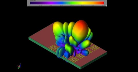
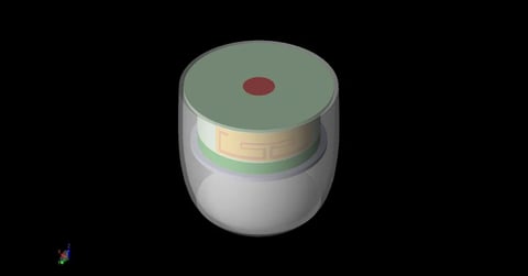
The example’s geometry is based on a simplified smartphone PCB. A 150x70x1 mm sheet of copper is used as the ground plane for the system with the antenna structures mounted on one end, as shown in Figure 1. The 4G antenna is placed directly over the ground plane in an inverted-L shape that has a 1x1 mm cross section and lengths of 6 mm on the short leg and 70 mm on the long leg. It is fed by a voltage source between the ground plane and the end of the short leg. The 5G array is comprised of four identical Yagi-Uda elements shown in Figure 2. The elements are mounted on a 0.3 mm thick substrate (dielectric constant = 3.6, loss tangent = 0.006) which is separated from the ground plane by a conducting block 2.2 mm thick. There is also a horizontal element of the Yagi-Uda antenna on the back side of the substrate which is visible in Figure 3. Each 5G element is fed by a Nodal Waveguide source.
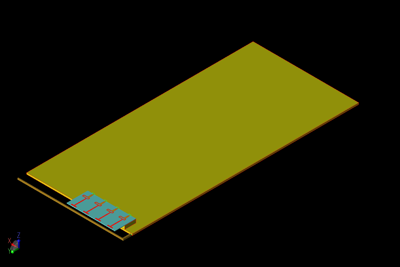
Figure 1: The smartphone design is shown in a three-dimensional CAD representation with the 4G antenna and 5G array structures visible at the left on one end of the large ground plane.
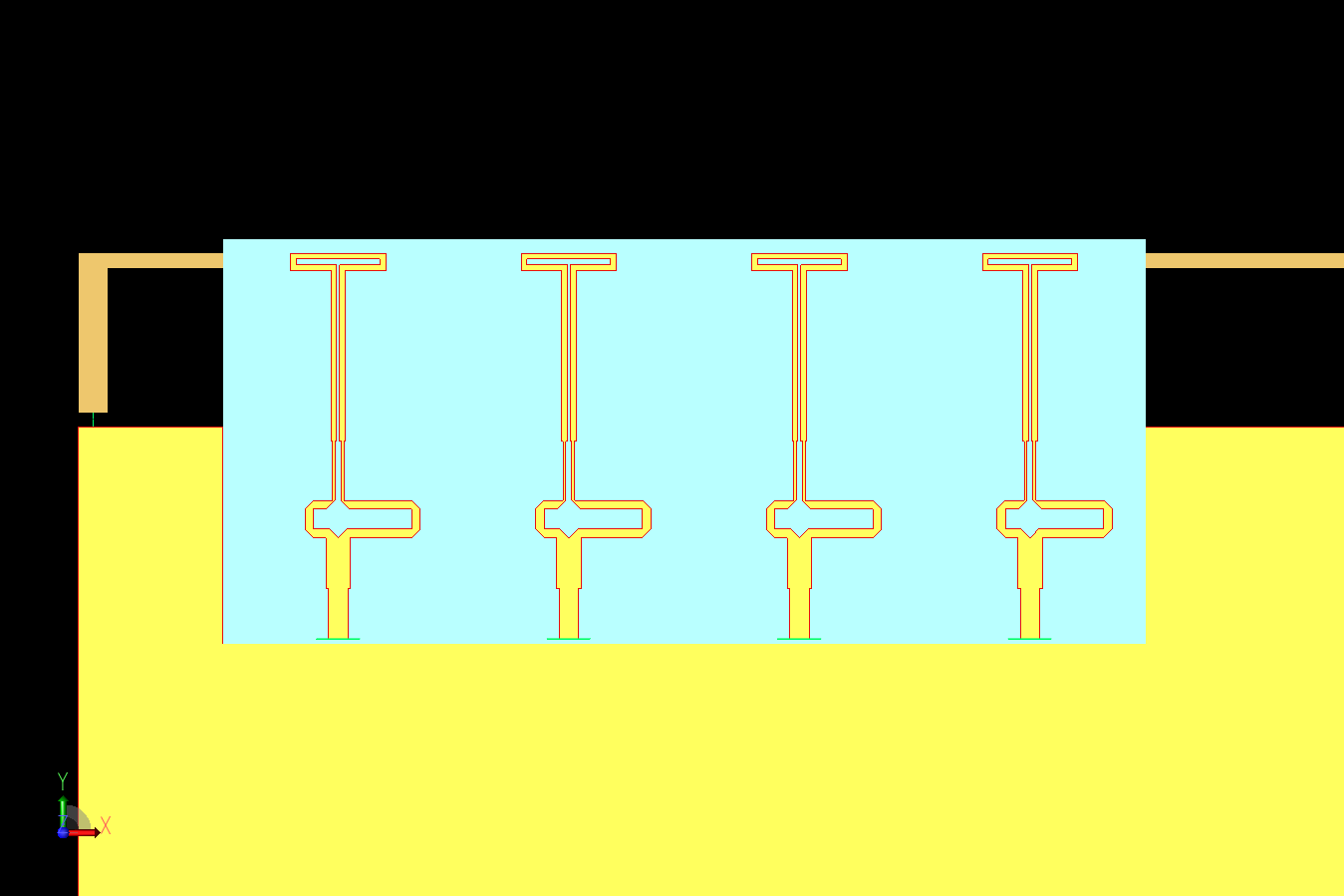
Figure 2: A CAD view of the 5G array showing the four Yagi-Uda elements on a dielectric substrate with the 4G inverted L antenna behind.
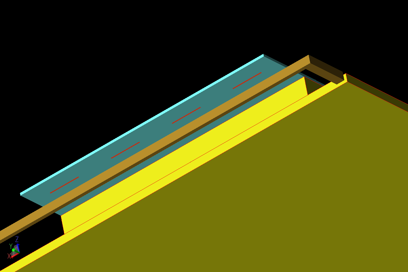
Figure 3: An underside view of the antenna array shows the separation of the 4G and 5G elements and the back side of the substrate.
The structure is meshed using the PrOGrid Project Optimized Gridding® feature of XFdtd with a base setting of 30 FDTD cells per wavelength. Minimum feature sizes are defined to ensure the substrate has five FDTD cells of thickness and the smallest conductor features are five cells across. Automatic fixed points are also applied to all parts to ensure grid lines are placed on all the edges of the geometry.
Results
The 4G antenna is fed by a broadband source which is initially represented as a 50-ohm voltage source attached between the ground plane and the antenna base. The antenna is not a good match to the 50-ohm source resulting in poor return loss. After an initial simulation to determine the impedance of the antenna load, a matching circuit can be defined to improve the antenna performance. In this case, a lowpass-PI matching network consisting of two capacitors and an inductor is selected for use and component values are determined using analytic matching circuit calculators. The matching network components are defined in a SPICE netlist format and then imported into XFdtd as a sub-circuit as shown in Figure 4. This sub-circuit can then be added to an XFdtd voltage source as a matching circuit (Figure 5). During the execution of the program, a co-simulation of the FDTD full wave calculation and a circuit solver takes place for each time step at the cell edge containing the matching circuit. A normal full wave FDTD simulation takes place for the remainder of the calculation space. The resulting return loss plots for the unmatched and matched 4G antenna are shown in Figure 6 and the marked improvement from the matching circuit is visible. The gain of the 4G antenna is shown in Figure 7 and can be seen to be provide broad coverage with a peak gain of 2.7 dBi.
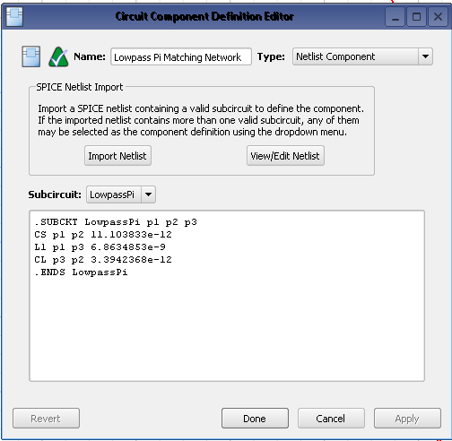
Figure 4: The menu for the netlist of the matching circuit used in the 4G antenna is shown. The netlist contains two capacitors and one inductor.
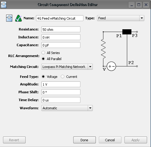
Figure 5: Shown is the voltage source menu in XFdtd for the port with the matching circuit that is used for the 4G antenna.
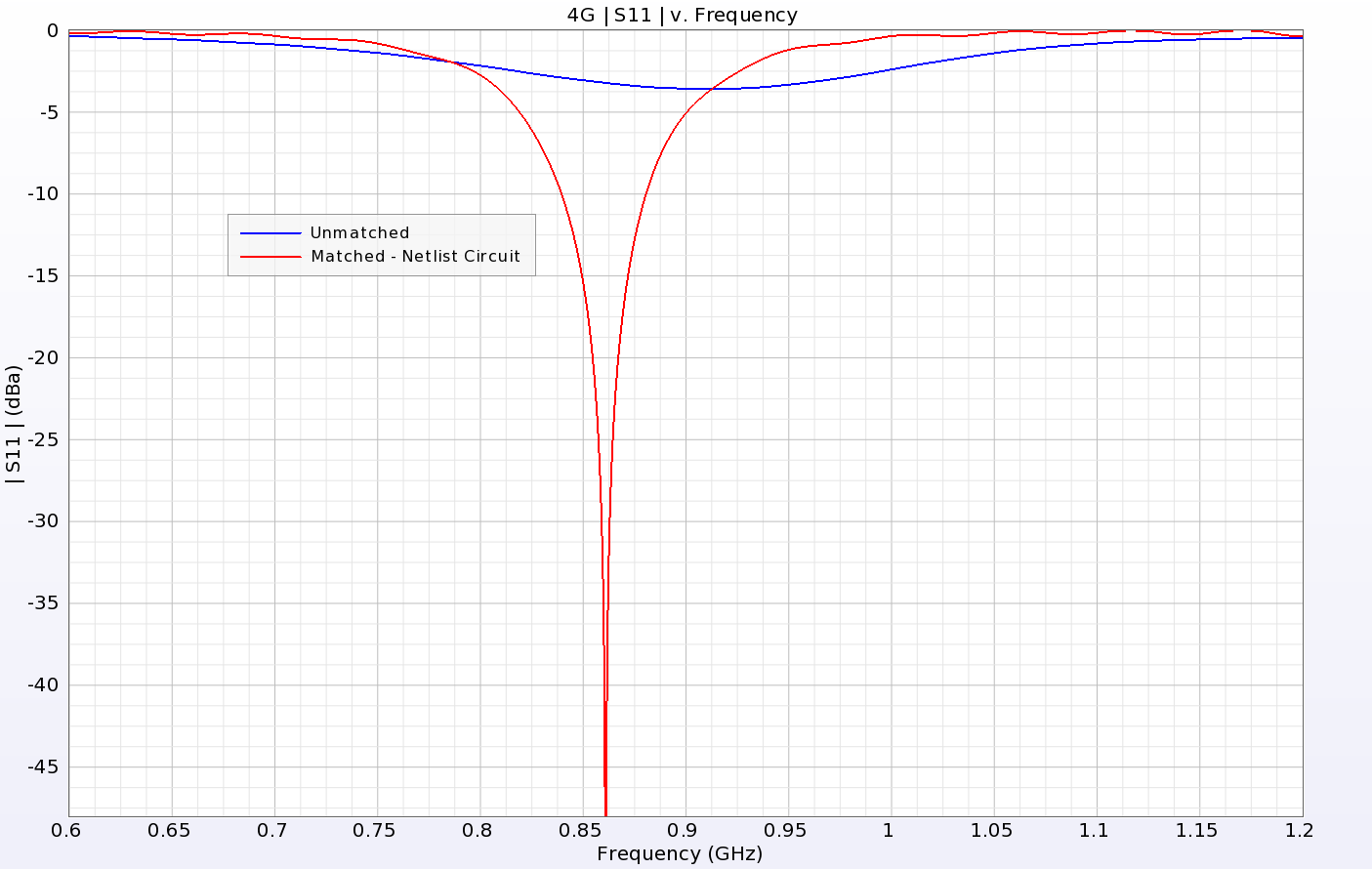
Figure 6: Return loss comparison for the unmatched and matched 4G antenna.
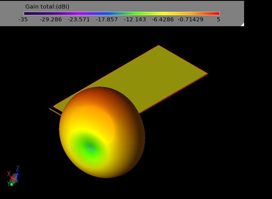
Figure 7: The 3D gain pattern of the 4G antenna shows fairly uniform coverage around the device and a peak gain of 2.7 dBi.
The orientation of the 5G antenna array relative to the 4G antenna is varied to determine the impact of the positioning on the performance of each antenna. Three configurations are considered and are shown in Figure 8: shift the 5G array so the tops of the 5G antennas are 2 mm below the top of the 4G antenna, keep the tops of the 5G and 4G antennas at the same level, or shift the 5G array up by 2 mm. In these initial cases, the phase shift between the 5G array elements is kept at zero. The impact of the offset is displayed in Figure 9 and Figure 10 where it can be seen that the offset of the 5G array down by 2 mm has a noticeable impact on the gain pattern in both the XY and YZ planes. Moving the 5G array up by 2 mm produces a pattern similar to when the 4G antenna is completely removed from the geometry. When the tops of the 4G and 5G antennas are aligned, there is a slight impact to the 5G antenna pattern. In all cases, the 4G antenna pattern is only slightly impacted, as can be seen in Figure 11.
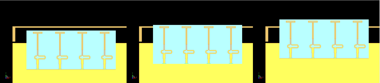
Figure 8: Three different configurations of the 5G array relative to the 4G antenna are considered (left to right): an offset of the top of the 5G antennas 2 mm below the 4G antenna, even alignment between the top of the 5G antennas and the 4G antenna, and an offset of the top of the 5G antennas of 2mm above the 4G antenna.
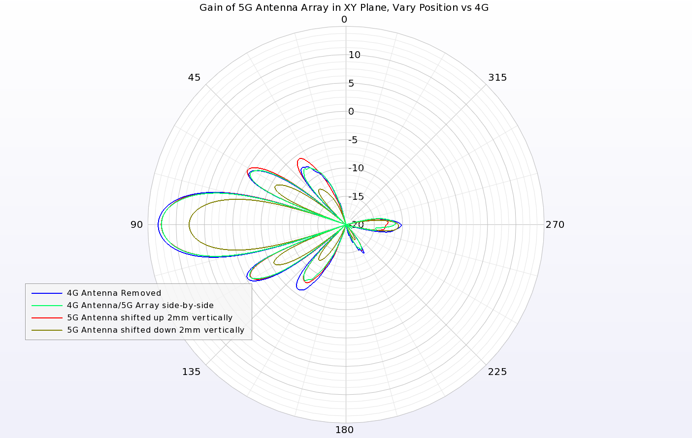
Figure 9: Plots of the gain pattern in the XY plane of the 5G array with zero phase shift between elements are shown. It can be seen that with the 5G array offset by 2 mm above the 4G antenna, the pattern is similar to when the 4G antenna is removed from the geometry. Similar patterns are found when the tops of the 4G and 5G antennas are aligned. When the 5G antennas are offset 2 mm below the 4G antenna, the 5G pattern is significantly affected.
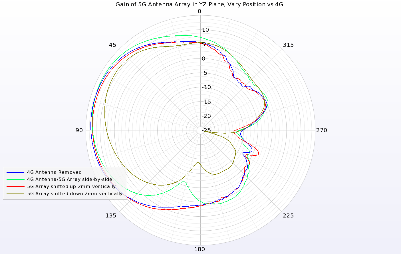
Figure 10: Plots of the gain pattern in the YZ plane of the 5G array with zero phase shift between elements show similar results for the 2mm above offset to the case of the 4G antenna removed. There is some impact on the 5G array pattern when the tops of the antennas are aligned and a larger impact when the 5G antennas are shifted 2 mm below the 4G antenna.
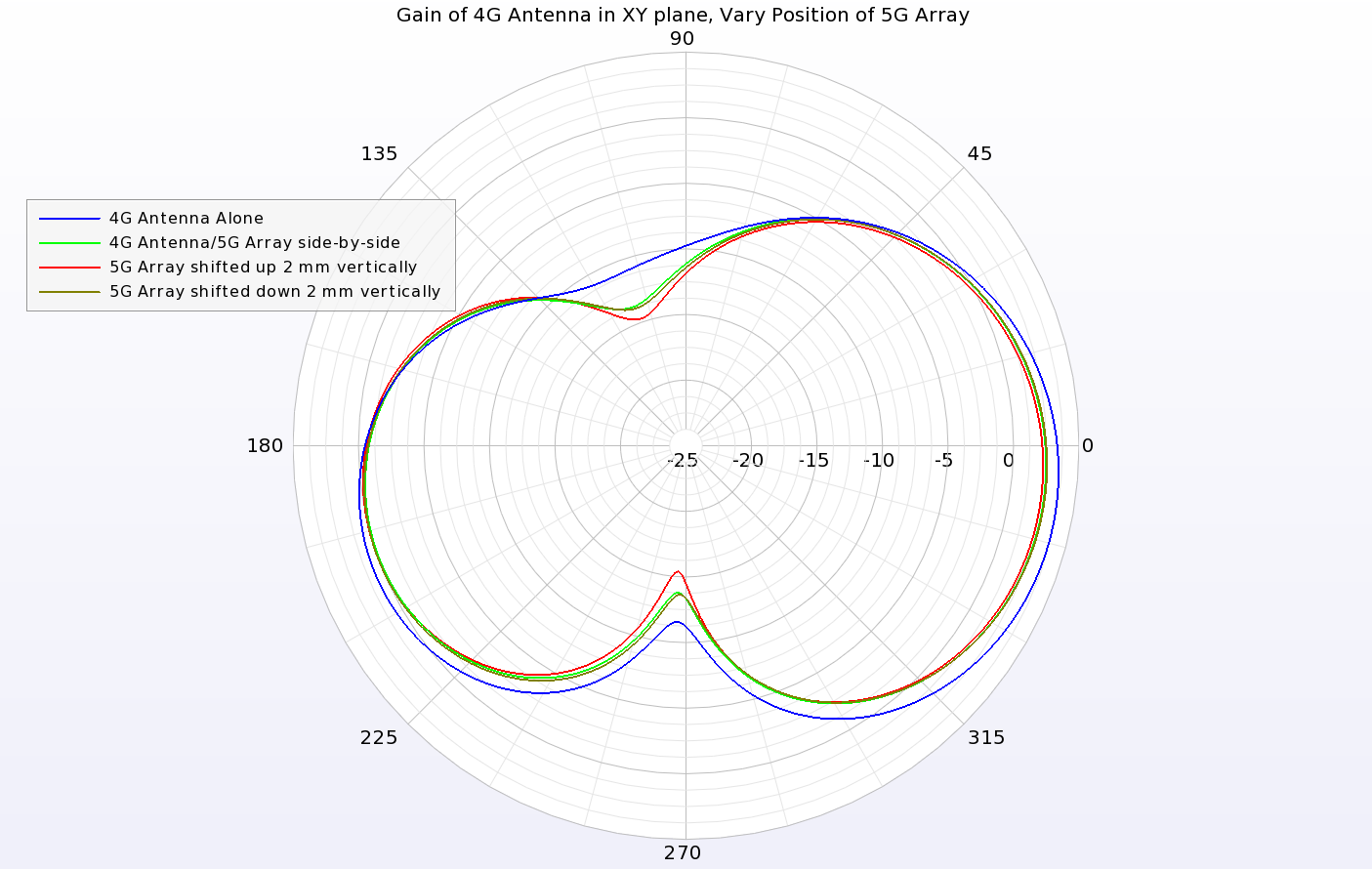
Figure 11: The gain pattern of the 4G antenna in the XY plane is only slightly impacted by the movement of the 5G antenna array.
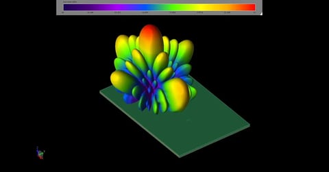
Next, the 5G antenna array is fed by a 28 GHz sinusoidal source with equal amplitude and a variable phase shift across the elements for the configuration where the 5G array is positioned 2 mm above the 4G antenna. With the array fed with all elements in phase, the pattern produced has a peak gain of about 12.5 dBi with a 3 dB beamwidth of 17 degrees and a peak sidelobe level below 0 dBi (Figure 12). After applying a phase shift of 120 degrees between each element of the 5G array, the beam is scanned 24.5 degrees to one side as shown in Figure 13. Applying phase shifts of -180, -120, -60, 0, 60, and 120 degrees to the feeds produces a series of beams from the array, shown in Figure 14 where all beams are plotted at the same time.
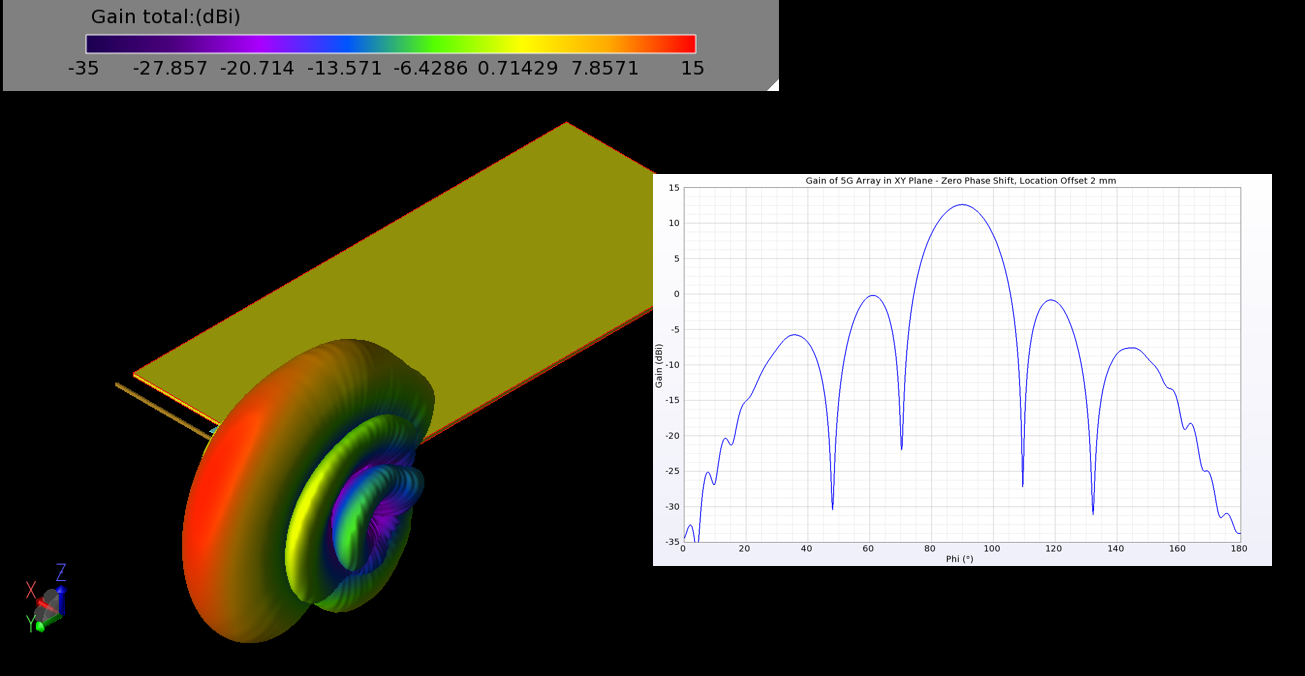
Figure 12: The gain pattern of the 5G array with zero phase shift between elements shows a beam with peak gain of 12.5 dBi and a beamwidth of 17 degrees in the XY plane.
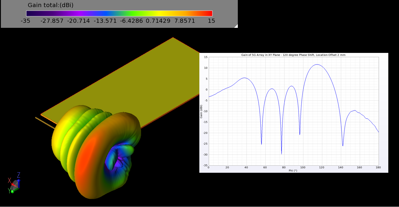
Figure 13: The gain pattern of the 5G array with a 120 degree phase shift between elements shows a beam tilted 24.5 degrees in the XY plane.
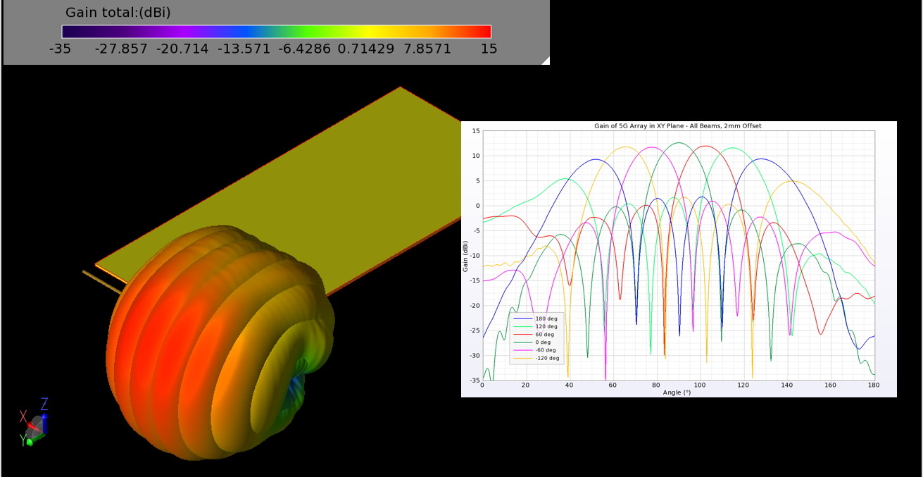
Figure 14: Six possible beams of the 5G array are shown in 3D and 2D gain patterns for the cases of a phase shift between elements of 180, 120, 60, 0, -60, and -120 degrees.
Summary
A simplified smartphone device with a 4G antenna combined with a 5G array at 28 GHz is evaluated for different configurations of the 5G array relative to the 4G antenna. A best-case configuration with the 5G antenna offset 2 mm vertically relative to the 4G antenna was found with results that indicate there is nearly no interaction between the 4G and 5G elements.
Reference:
[1] T. Yamagajo, Y. Koga, M. Kai, T. Tonooka, H. Sumi, and M. Hoshino, "A Nobel 4G and 5G Antenna Solution for Future Smartphones," IEEE Antennas and Propagation Society Int. Symp., pp. 1785-1786, 2018.